A US semiconductor startup founded by ex-Qualcomm employees is betting that its new class of edge server processor can meet increased demand for cost-optimised solutions to meet the demand for edge inferencing and vRAN solutions.
Kenyi Technologies is developing what it describes as an “edge server processor” – a chiplet-based platform designed to bring cloud-native software capabilities to telecom and enterprise edge environments while, it says, maintaining the cost and power efficiency of traditional purpose-built appliances.
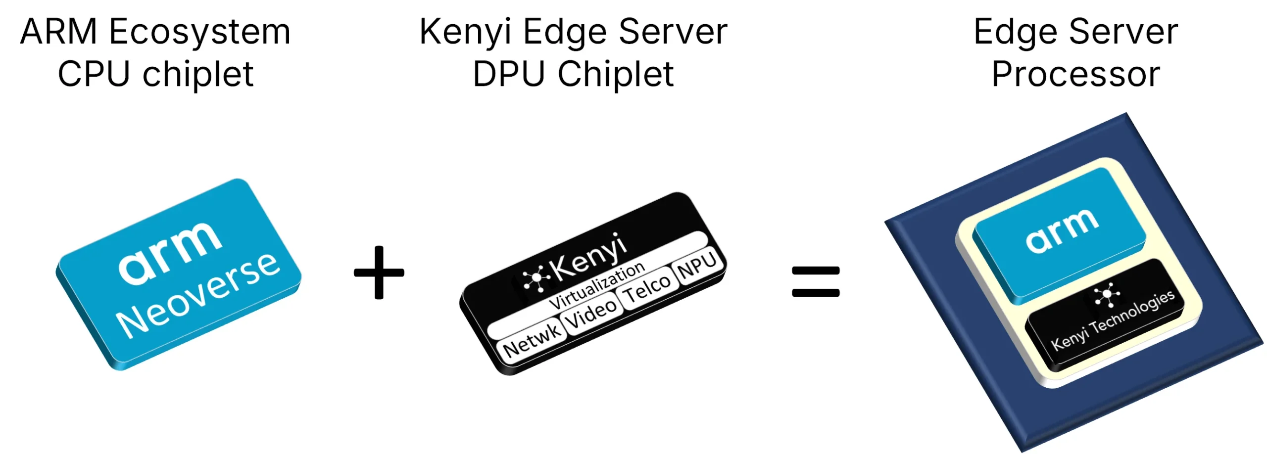
The Kenyi solution leverages chiplet technology to supplement an ARM Ecosystem Server Grade CPU with acceleration optimised for Edge Infrastructure use cases such as VRAN, Video Analytics and AI Inferencing.
Kenyi is raising a seed round to take the product to design closure and tape-out readiness. It recently announced it has received funding from SOSV and will be stationed at the SOSV HAX hard tech program in Newark, NJ. It also announced a strategic MoU with ADTechnology to co-develop a Server Processor solution that combins Kenyi Technologies Edge DPU chiplet platform with ADTechnology’s 2nm ARM-based CPU to form an integrated Edge Processing solution.
By combining a server grade ARM CPU chiplet with a DPU accelerator chiplet, Kenyi said the solution could improve power efficiency and scalability of vRAN Distributed Unit (DU) solutions at cost points commensurate to legacy purpose-built appliances, as well as provide a framework for proximal inferencing offload to Edge Infrastructure in a cost-effective manner.
About Kenyi
Kenyi was co-founded in 2024 by CEO Vincent Loncke and now has nine staff. Loncke was an early employee at Flarion Technologies, the OFDMA pioneer acquired by Qualcomm in 2006, and spent years inside Qualcomm working on infrastructure platforms and accelerator architecture for telecom workloads, including a spell as architecture lead on Qualcomm’s QX100 modem, which was targeted at O-RAN radio vendors.
Speaking to TMN, Loncke said he left Qualcomm in February 2024 with a small group from his team to launch the business, aiming to address what he saw as a major shift underway in network infrastructure: the move away from proprietary purpose-built silicon and toward commercial off-the-shelf, software-defined platforms.
“We’re building the future of RAN chipsets and hardware,” he said.
The problem: telcos want flexibility, but not higher costs
In Loncke’s telling, although specialised hardware appliances from vendors such as Ericsson, Nokia and Samsung are highly efficient, they are expensive, proprietary and difficult to adapt for new workloads such as AI inference and 6G-era services.
As a result, the industry has been pushing toward virtual RAN (vRAN) and Open RAN architectures, where network functions run increasingly in software on general-purpose servers.
The challenge, according to Kenyi, is that generic servers – especially GPU-heavy systems – often fail the economics test for telecom operators.
“Telcos are very cost sensitive,” Loncke said. “It’s cost, cost, cost — capex, opex, power per watt.”
Rather than asking operators to dramatically increase spending to support speculative AI workloads, Kenyi says it is designing a platform that fits within existing infrastructure refresh budgets. Its website describes the goal as delivering “cloud native software stacks with appliance-like efficiency in terms of cost, power and space.”
Kenyi hopes to build a cost-efficient platform to meet edge use cases such as AI inferring to meet potential new use cases.
What Kenyi is bringing to market – focus on the DPU layer
At the centre of Kenyi’s strategy is a chiplet architecture formed via its relationship with Arm, whose Neoverse and newly announced AGI CPU roadmap is increasingly focused on infrastructure and AI workloads.
Arm recently introduced its AGI CPU as its first production silicon, aimed at high-efficiency AI infrastructure and based on Arm Neoverse CSS V3. Kenyi says its DPU is designed to complement this kind of platform by adding the edge-specific acceleration needed for telecom and distributed AI use cases. This approach allows Kenyi to avoid building a full server ecosystem from scratch. Instead, it can rely on established Arm-compatible server manufacturers while focusing its own engineering effort on the differentiated DPU layer.
The platform combines an Arm-based server-grade CPU chiplet with a proprietary Kenyi DPU (data processing unit) chiplet containing hardware accelerators tailored for edge workloads. These include telecom functions such as forward error correction (FEC), Fast Fourier Transforms (FFT) processing and networking acceleration needed for vRAN, alongside support for video analytics, data analytics and secure enterprise AI services.
The result is a single-package edge server processor designed to serve multiple use cases, with telecom as the lead vertical.
Loncke says, “We have an MoU with Arm to co-develop this platform. If you look at Arm’s recent announcements, they announced AGI, built primarily for Meta as a lead customer, but they’re going to offer that as a cloud CPU. For Arm, it’s a transition: up until now it has been an IP provider. They’ve sold their CPU IPs to Nvidia, Qualcomm and so forth. So this is a foray for them into merchant silicon.
“What we’re going to do is use chipsets to build a DPU (Data Processing Unit) that has accelerators in it that are tailored for the edge, as opposed to running it all in the CPU. So we provide those accelerators in our DPU. That constitutes our Edge Server platform.
“Telco is not the only use case that we’re looking at. There’s networking use cases, there’s video, there’s use cases at the edge where data sovereignty is important and enterprises don’t want to send data to the cloud. So it’s a broader set of use cases. But telco is our lead use case.”
Kenyi ‘s DPU provides “lookaside” acceleration for vRAN – a model where specific modem functions are offloaded to accelerators while the rest of the radio stack remains software-defined on the CPU. Loncke argues this approach is winning industry support over “inline” accelerator designs because it preserves software flexibility and reduces vendor lock-in.
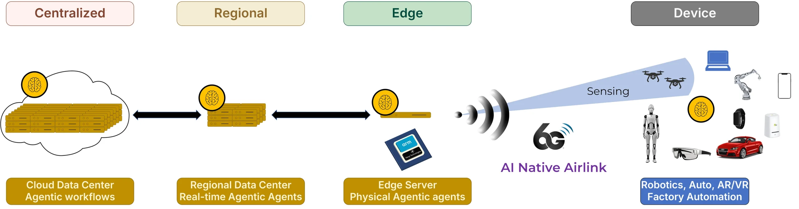
The company sees this as essential for enabling future 6G workloads and low-latency AI inference close to the user.
There’s an irony here as Loncke was architecture lead on the Qualcomm X100 accelerator solution which advertised inline processing as its advantage – essentially “a dedicated modem that you’re plugging into PCIe” that handles the entire Layer 1radio processing in hardware rather than leaving most of it in software on the CPU. Although he is reluctant to go into too much public detail over Qualcomm’s decision, it’s clear that he now feels that lookaside is the better architecture for vRAN.
He will say, “Large companies that have legacy tend to build based on what their DNA is. In vRAN Intel wants a CPU, Nvidia wants a GPU and what Qualcomm is going to do is going to do is take the UE modem, make a bigger version and make that their vRAN.”
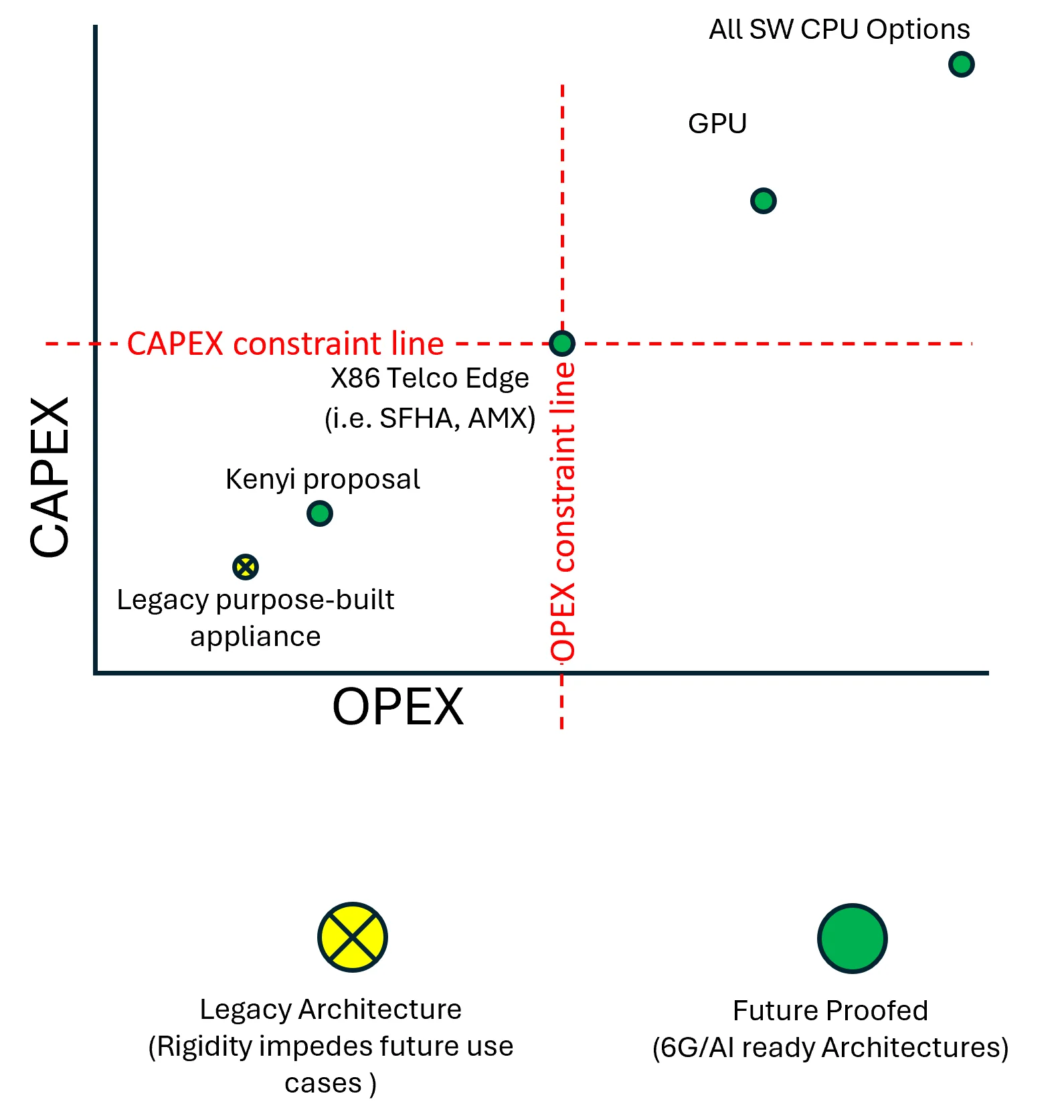
How Kenyi positions its solution against over vRAN platform options
From stealth to seed stage
Kenyi demonstrated an FPGA-based proof of concept at Mobile World Congress 2026 showing power-efficiency gains for Arm-based vRAN versus x86 infrastructure, and says it plans to use this as a route toward deeper engagement with major telecom ecosystem players.
Its route to market will rely heavily on server manufacturers and software integrators rather than direct operator sales. The company expects the hardware to flow through the Arm ecosystem into server vendors, while telecom software integrators such as Ericsson and Samsung remain critical because they control the software stacks operators deploy. But as this video makes clear, Kenyi thinks that the growth of an AI-native 6G air interface and the growth of edge inferencing applications will require an edge platform that sites between the speculative economics of a GPU-based AI grid, and the inflexibility of an appliance-based RAN.